INTEGRATION OF MEMS COURSES INTO AN ENGINEERING CURRICULUM
ABSTRACT
Microelectromechanical systems (MEMS) is a relatively new, rapidly growing area of research and development and commercialization, that may ultimately rival integrated circuits in importance. In order to respond to the need for improved education in MEMS, three courses have been introduced at the undergraduate level in a new curricula in Microelectromechanical Systems. Specifically: Microdevices and Micromachining Technology, Materials for MEMS, and Microactuators. The goal was to prepare students for the interdisciplinary field of MEMS with a series of intensive courses and encourage enrollment across the College of Engineering. The laboratory course in microdevices and micromachining technology includes a series of skill-building experiments, to introduce the fundamentals of microfabrication processes. As the capstone projects in this course, students fabricate either a pressure sensor or a glucose sensor. A new laboratory infrastructure was established for the class and the costs are reviewed. Enrollment was across the engineering disciplines and the students were successful in gaining competency in the laboratory skills and an understanding of the fundamental principles. Feedback from students was enthusiastic about the experience of building a functioning device in the semester course.
INTRODUCTION
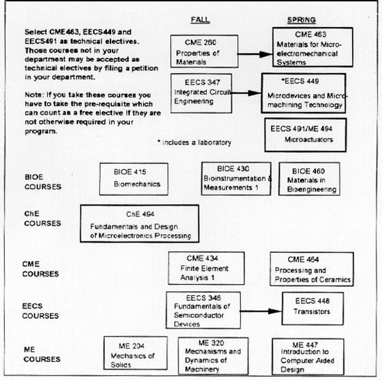
Micromachining is now a well established technology for the manufacture of miniature pressure sensors and microaccelerometers and is beginning to find important uses in bioanalysis. Although there has been steady growth of research activity in this field[1,2] in microsensors, microfabricated systems[3,4] and microelectromechanical systems[5,6], there is a distinct lack of curriculum at the undergraduate level addressing these topics. A limited number of classes have been introduced in some programs at the graduate level at MIT[7] and Dartmouth College[8], the University of Minnesota, Stanford University and the University of California at Berkeley. The essence of the curricula developed at UIC is to allow undergraduates in traditional engineering disciplines to take a minor concentration in MEMS. Table 1 shows the senior year course selections available for a concentration in MEMS at UIC. These courses also provide a solid foundation for a MEMS research program.
Over the past few years, four new courses in MEMS have been introduced in the Electrical Engineering and Computer Science (EECS) Department, one in the Mechanical Engineering (ME) Department, one in the Civil and Materials Engineering (CME) Department, and one in Chemical Engineering (ChE). Our objective is to increase the quality and quantity of laboratory experience by introducing a series of skill building experiments followed by a capstone project which combines the skills from earlier components in the course. In addition, we use a problem solving approach, to approximate real world design and engineering problems which involve some uncertainty, trade-offs and priorities, supplemented with case studies, rather than the traditional approach of dissecting a subject into its component parts. This provides strong motivation for the students to study based upon the objective of solving the problem effectively and provides a "reality check" by linking the material to a particular application. Students are drawn from five different departments to participate in this program.
TABLE 1: CURRICULUM IN MEMS INTRODUCED AT UIC up
The point for introduction of the laboratory course could either be at the beginning of the senior year or in the junior year. The advantage of a senior level laboratory course is that the students would be able to implement a senior design project in the Spring semester. However, sufficient time for prerequisites, such as a course involving basic integrated circuit fabrication techniques, must be implemented, before the MEMS course would occur in the last senior year academic term.
PREREQUISITES
The issue of prerequisites for MEMS courses is an important one. Prerequisites for MEMS courses must include a materials science course in addition to the usual physics, chemistry, mathematics, and computer courses which are included in most first and second year engineering curricula. The difficulties of having students from disparate backgrounds means that prerequisites have to be selected carefully. For example, ME and ChE students without a semiconductor fabrication background are at a disadvantage to EE students. Similarly, EE students and ME students without thermodynamics from a materials perspective are hindered with respect to Materials Science and are at a disadvantage when dealing with thermal, stress, and mechanics issues. Since most MEMS science and technology has evolved from EE, students from ME, ChE and perhaps Materials Science may need more help with device physics and silicon processing, including an early introduction to the terminology of semiconductors (VLSI, CMOS, etc.).
COURSE CONTENT
The content of the MEMS courses should be selected so that it is as fundamental and as broad as possible to accommodate students from all of the engineering disciplines, as well as physics majors. This concept will minimize the requirement for specialized courses, and it will promote academic cross-fertilization between the disciplines. A primary point is that MEMS classes should emphasize the fundamental science and technology concepts. It is important that each student must attain a level of understanding so that they can address a complex design problem. At the same time, the fundamental science and technology of MEMS must be presented to allow a long-term understanding of the fundamental concepts. Thermodynamics, the effect of scaling on mechanical and interfacial forces, and properties of interfaces, are fundamental to MEMS education.
Microelectromechanical systems envelope a vast range of materials and fabrication processes and necessarily attracts students with varying technical backgrounds. Because of this, the lecture portion of any course must be quite broad, and the instructor may have to sacrifice technical depth in order to cover a sufficiently wide range of topics. The emphasis of the lectures should be focused on the fundamental physical and chemical science concepts which underlie the MEMS technology. It is also recognized that the details of the course structure and topics covered may vary among institutions in response to local interests and conditions. Nevertheless, the key issues that should be included in a microelectromechanical systems course include:
1. Knowledge of the individual processing steps necessary to microfabricate MEMS
devices
and how these steps can be integrated to produce a final device.
2. Understanding of the physical scaling issues concerning MEMS devices and the
significance of the interfacial phenomena in high surface-to-volume ratio microdevices.
Due to the interdisciplinary nature of MEMS, and since there are at present so few CAD
tools
for MEMS device design, the ability to do lumped system modeling and analysis is crucial. This
ability will require EE's, for instance, to learn more about thermal and mechanical system
modeling than is usual for typical EE systems courses. In addition, appropriate use of software
design tools, such as SUPREM III, (and possibly SUPREME IV) or computer codes developed
by our groups for microelectronic processes, augment or supplement laboratory experiments.
In general, it is valuable for students to have direct hands-on experience in a microfabrication laboratory. It is also valuable to utilize outside fabrication resources, such as MCNC (Center for Microelectronics Research Triangle Park, North Carolina). It is particularly important for students to have the experience of fabricating and testing a functional MEMS device at the conclusion of the course to fix their long-term interest in this technology.
MATERIALS FOR MEMS
This course builds on the introductory Properties of Materials course (CME 260) which is taken at the sophomore level by many engineering students. It is offered to advanced undergraduates and graduate students, and addresses the specific material and material processing issues which are likely to be encountered in MEMS technology. The course is similar to many electronic materials courses, but because these courses often focus on semiconductors and/or electronic ceramics, no single textbook has been identified which covers all of the subjects which are addressed. Course material is drawn from recent literature as well as several electronic materials texts.
After a brief review of fundamental materials concepts, the course addresses silicon processing and wafer production, oxidation to form SiO2 films, CVD of ceramics and metals. The effects of process parameters on structure and properties of film is emphasized. A thermodynamics section addresses phase equilibria in systems relevant to metallization (silicides and alumides). Electroplating and electroforming are discussed in the context of the LIGA process for microdevice fabrication. A later section of the course addresses dielectrics, ferroelectrics, and piezoelectric ceramics in the context of microsensors and actuators. There is a brief discussion of shape memory alloys. There is presently no formal laboratory requirement in the course, although demonstrations and plant visits have been used in the course as appropriate.
The course has been taught to both graduate and undergraduate students from the Metallurgy, Materials Engineering, Chemical Engineering, Electrical Engineering, Mechanical Engineering and Applied Physics programs.
MICRODEVICES AND MICROFABRICATION TECHNIQUES
The rationale for introducing the Micromachining and Microdevices (EECS449), course was to prepare students for the interdisciplinary field of MEMS with an intensive laboratory experience supplemented with class room instruction. Enrollment was across the College of Engineering, see Table 2. Students who go on to graduate school in areas requiring fabrication skills are able to become productive much more rapidly than students who have no hands-on experience in fabrication. The prerequisite for the class is a lecture course in Integrated Circuit Engineering (EECS 347) which prepares the students with the basic principles of integrated circuit (IC) fabrication, including: photolithography, vacuum systems, etching, diffusion, and introduces students to the terminology used in IC engineering [or a course with emphasis, for example, on thermodynamics, chemical kinetics, reactor design, optimization, and other engineering principles and concepts as they apply to microfabrication techniques (e.g., ChE 494 "Fundamentals and Design of Microelectronics Processing")] . This allows us to begin the course with an intensive laboratory component which focuses on the fabrication processes they have studied in EECS347. The students design and fabricate a functioning microsensor using the processing techniques they have learned. The lecture component focuses on the fundamental principles of microsensors and uses two case studies for in-depth analysis and design: (1) a piezoresistive pressure sensor and (2) a glucose sensor.
| TABLE 2: STUDENTS ENROLLMENT up, down | |||||||||||
| Year | Course | Undergraduate | Graduate | Total | |||||||
| CME | EE | ME | ENG
PHY |
CHE | CME | EE | ME | PHY | |||
| 1993/4 | EECS594* | - | - | - | - | 1 | 2 | 3 | 1 | 1 | 8 |
| 1993/4 | CME463 | 4 | 1 | 0 | 0 | 0 | 4 | 1 | 1 | 0 | 11 |
| 1994/5 | EECS491 | 0 | 5 | 0 | 0 | 0 | 0 | 4 | 0 | 0 | 9 |
| 1995/6 | CME463 | 0 | 0 | 0 | 3 | 2 | 4 | 0 | 0 | 0 | 9 |
| 1995/6 | EECS449 | 0 | 3 | 0 | 0 | 0 | 1 | 2 | 2 | 1 | 9 |
| 1996/7 | EECS449 | 0 | 5 | 0 | 1 | 2 | 1 | 2 | 2 | 3 | 16 |
* offered as graduate course
A microfabricated pressure sensor was chosen because it is a straight forward device that utilizes many of the principles manifest in MEMS. The importance of stress analysis for the diaphragm design and the electrical measurement principles are melded into one device. The fabrication processes are the same as those utilized to produce many more complex MEMS devices. Microfabricated silicon pressure sensors are also a very successful commercial product and a good foundation of research has been carried out on the device design and operation[9,10,11,12]. The design used here consists of a p+ silicon membrane formed by an etch stop, with polysilicon strain gauges sputtered on two edges of the membrane to detect deflections.
The glucose sensor[13] was selected because it is one of the most important biosensors and is straight forward to fabricate and to understand its operation. The primary objectives of the laboratory course are for students to carry out fabrication processes, however there are a limited set of processes that can be most effectively implemented by the laboratory technician or TA. In particular, processes that utilize delicate equipment, that involve critical safety issues, or equipment that have high maintenance costs. The students can then focus their attention on those processes which are simpler to accomplish, as well as the performance testing of their finished MEMS devices.
A grant from the National Science Foundation, with matching funds from the EECS, ME Dept. and Office of the Vice Chancellor, has allowed us to convert our existing clean room to a Student Microfabrication Laboratory (SML) to support the new courses, senior design, and undergraduate research projects. This laboratory clean room is separate from the Microfabrication Applications Laboratory, which is primarily a research facility. The total cost of equipment has been considerable. In the first year of the grant, $100,000 [1993 dollar value] enabled us to purchase an Infrared Mask Aligner, Thermal Evaporation Station, Inspection Microscope, and Anisotropic Etching Tanks. The undergraduate laboratory committee has been very supportive of this program with assistance for additional equipment of $35,000 in 1993 for microscopes, probe stations, 486PC's, ovens, and $35,000 in 1994 for a wet bench, soft-wall clean room and quartz ware. A detailed breakdown of the equipment expenditures is given in Appendix A. Most universities have not been able to set up a separate microfabrication teaching laboratory, but with the drop in prices for prefabricated clean rooms and equipment it is now possible to do so at a reasonable cost. The department is currently providing staff for the SML and covers the cost of materials and supplies used in the instructional courses which has amounted to approximately $7,000 each year for the past two years, and $2,500 this year. We anticipate that the annual cost will be lower in subsequent years because many of the materials and supplies are bought in bulk quantities and only a fraction is used each time the course is offered. The laboratory has a higher budget than any of the other instructional courses in the department. The cost of equipment maintenance is currently being shared between the MAL and the EECS Dept. Based upon our experience over the past four years we estimate the annual cost at approximately $5,000. Additional costs and activities include: modifications to the structure of the room for installation of the clean hood, cost of soft wall clean room and chemicals, complying with the safety requirements putting together of material safety sheet, safety supplies, ordering of chemicals and materials which are not normally used in an electronics laboratory, labeling of the waste chemicals, maintenance for furnace tube and loading elephant, heating plate for the bubbler, and coordination with the health and safety department at the University.
For anyone planning to set up such a facility, one needs to consider the existing infrastructure at your University. In our case there is a Microfabrication Applications Laboratory which has technical support staff who we can draw on for assistance with the teaching laboratory. In addition, all the equipment used in the laboratory class is duplicated in the MAL facility, so that if there was a breakdown in at a critical time, the laboratory experiments can continue more or less as planned. If this was not the case one might consider having additional experiments ready that can be done in-place of the one originally scheduled.
In its current form the course as EECS449 with a mix of students as listed in Table 2. The students attend two lectures per week of 75 min. duration and a 4 hour laboratory. In the laboratory the first seven experiments covered the basic skills of oxidation, photolithography, etching and metallization, as listed in Table 3. The text book was Microsensors by Gardner1 and several referenced texts were used [14,15 ]. Students were made aware of the safe handling of chemicals and precautions to prevent contamination when using the diffusion and oxidation furnace. For each experiment students were given a detailed write-up providing theory and a background for the process, detailed step-by-step processing procedure, and homework problems based upon the theory in the laboratory. In each laboratory section the TA and faculty member were present. The full text of the laboratory manual is available on the World Wide Web at http://www.eecs.uic.edu/~peter/eecs449/.
| TABLE 3: LABORATORY EXPERIMENTS up | |
| Week 1 | Chemical safety training |
| Week 2. | Wwafer cleaning and oxidation of silicon |
| Week 3. | Photolithography |
| Week 4. | Oxide etching |
| Week 5. | Silicon anisotropic etching |
| Week 6. | Thermal evaporation of aluminum and lift-off photolithography |
| Week 7. | Silicon to glass anodic bonding |
| Week 8-14. | Class project |
A) Determine diffusion parameters
|
The students are required to fill in the blanks with their desired process parameters. Then during the laboratory session the actual process conditions used are recorded and any deviations from the planned procedure. The procedure shown is one of the most complex in the laboratory course. We have selected this one because it illustrates an important aspect of the TA's function: to keep the procedure within the laboratory period of four hours to achieve this the TA carries out several parts of the process. In particular: C) activation of sources which is a standardized procedure, and F) removal of the oxide layer which requires the use of a concentrated acid and is carried out by the TA under the supervision of the faculty member.
FOUNDRY MODEL
The Multi-User MEMS Process (MUMPS) at MCNC is a fabrication service offered four to five times per year based upon a three layer polysilicon process. It is designed to provide maximum user flexibility and low-cost access to MEMS process technology for the domestic industry, government and academic communities. In addition, the CaMEL Element Library helps novices and experts design MEMS devices using predefined micromechanical elements, allowing the user to assemble them into custom MEMS systems. These fabrication services are a most effective method for introducing MEMS since it required minimal knowledge of the fundamental processing technologies. If possible, students should implement a basic surface micromachining process in their own laboratory and this hands-on experience would provide the students with valuable insight into the fabrication process to sharpen their design skills for a MEMS project via MUMPS. Acknowledging the difficulty in teaching and learning the MEMS software design tools and the complexity of a three-layer polysilicon process, the pre-fabrication process which MCNC has recently introduced, facilitates realizing simple MEMS structures. In addition, preliminary devices could be fabricated in advance of teaching the course by the instructor to provide the students physical examples of devices, to formulate an accurate assessment of typical MEMS structures in advance. For universities operating on the quarter system, two quarters are needed to implement the MCNC pre-fabrication service. For example, the MEMS devices might be designed in the first quarter and then tested in the second quarter. For universities operating on the semester system, the devices could be designed, fabricated and tested in the Spring semester. To summarize there is no single way to use the MCNC facility, i.e. the use will depend upon local considerations, and upon the particulars of whatever course uses MCNC. MUMPs allows entree into MEMS devices in several ways, and this flexibility allows for different levels of interaction, this makes the MCNC service a very attractive educational tool.
MICROACTUATORS
Actuators are transducers that convert electric, magnetic, chemical, thermal, or optical energy into mechanical energy using one of two general methods: (1) An active material inherently converts non-mechanical energy into mechanical energy. Examples include piezoelectric, magnetostrictive, and shape memory alloy materials; (2) Non-active materials are fabricated into machines whose components interact to transform non-mechanical energy into mechanical energy. Examples include electric motors, capacitive comb actuators, inductive coil elements, and thermally actuated bi-material plates. Students study the scaling of forces, from which they learn that machines used to accomplish a given function on the microscale are very different from their macroscopic functional counterparts. Indeed, the microscopic counterpart of a macroscopic machine is often an active material. Students were required to take CEMM 260, Properties of Materials, simultaneously with this course. The course begins with an introduction to stress and strain, primarily for the benefit of the EE students. Thermoelasticity is then covered. Piezoelectric and shape memory alloy materials are discussed after the students have covered crystallography in the CEMM 260 class. One-dimensional examples are used to teach the concepts. The students can readily extend these principles to multiple dimensions in advanced courses or in their professional employment. The mechanics of bending bimorph actuators are covered with respect to a generic (thermal, piezoelectric, shape memory) nonelastic strain. An overview of micromachining is given with particular emphasis on the issues related to the design and fabrication of electrostatic micromotors. Active materials and micromachines are classified based on the actuation energy density, power, frequency, force, displacement and efficiency.
TEACHING METHODS
A recurring theme in effective education is the need to capture a student's attention. An effective means to introduce undergraduates into the MEMS program is through a summer research assignments with a faculty or senior graduate student mentor.
Exposing the students to fabrication processes which were not optimized is a valuable learning experience. To encourage the students to practice and develop polished laboratory skills and techniques, a large fraction of a MEMS laboratory grade was allocated to the laboratory note book; specifically 40%.
Teaming of an EE and ME student to work on a collaborative paper or mini-project could motivate the students to learn from each other. Use of a problem solving approach has been found to be extremely effective in teaching. The students develop some quite elegant solutions to problems posed. Students were asked to determine what skills and knowledge they would need to solve a given problem. It would be really effective to have students present their collaborative work to their peers at the end of the course, perhaps in the form of a one day symposium.
CONCLUDING REMARKS
New courses have been introduced into a MEMS curriculum at the senior undergraduate/first year graduate student level. Students feedback from their end-of-course critiques indicate the importance of realizing a functional MEMS device is both motivating and fulfilling. We have achieved the three most important aspects of a laboratory course in MEMS:
New methods of publishing text books and course material will become more important in the important. The course laboratory manual is on the World Wide Web and the possibility of publishing a text book on CD-ROM format that can be updated frequently is another exciting opportunity.
ACKNOWLEDGMENTS
Comments from Professors Edward Kolesar, Jay Zemel, David Naylor, William Robbins, Ash Parameswaran, Mark Shannon, Paul Zavracky, and Albert Henning, are gratefully acknowledged. Financial support for this work was provided by the National Science Foundation, Grant #EEC-9315420 and the interagency Technology Reinvestment Program (TRP).
REFERENCES
1. J. W. Gardner, Microsensors, Principles and Applications, Wiley, Chichester, England, 1994.
2. S. M. Sze, Editor, Semiconductor Sensors, John Wiley, New York, 1994.
3. P. J. Hesketh, J. N. Zemel, and H. Hughes, (Editors) "Microstructures and Microfabricated Systems," Softbound Proceedings of the ECS, Vol. 94-14 (The Electrochemical Society, New Jersey, 1994).
4. D. Denton, P. J. Hesketh, and H. Hughes, (Editors) "Microstructures and Microfabricated Systems - II," Hardbound Proceedings of the ECS, Vol. 95-27 (The Electrochemical Society, New Jersey, 1995).
5. Proceedings of IEEE International Workshop on Micro Electro Mechanical Systems, Amsterdam, the Netherlands, Jan.-Feb. 1995, IEEE Catalog Number 95CH35754, Piscataway, New Jersey.
6. Proceedings of IEEE International Workshop on Micro Electro Mechanical Systems, San Diego, Feb. 1996, IEEE Catalog Number 96CH35856, Piscataway, New Jersey.
7. A. K. Henning and C. G. Levey, "The science and technology of micro-machines: development of an undergraduate course," Proc. Eleventh Biennial University/Government/Industry Microelectronics Symposium, (IEEE, Piscataway, NJ, 1995), pp. 230-236.
8. M. Lu and M. A. Schmidt, "A process design course utilizing micromechanical devices," Proc. 9th Biennial University/Government/Industry Microelectronics Symposium, Melbourne, FL. June 1991, pp. 60-63.
9. S. Clark and K. Wise, "Pressure Sensitivity in Anisotropically Etched Thin-diaphragm Pressure Sensors." IEEE Trans. Elect. Dev., vol.ED-26, no. 12, 1979, pp. 1887-1896.
10. O. Tufe, P. Chapman, and D. Long, "Silicon Diffused-Element Piezoresistive Diaphragms" J. Appl. Phys., vol 33, no. 11, 1962, pp.3322-3327.
11. O. Tufte, and E. Stelzer, "Piezoresistive Properties of Silicon Diffused Layers." J. Appl. Phys., vol. 34, no. 2, 1963, pp. 313-318.
12. W. Pfann, and R. Thurston, "Semiconducting Stress Transducers Utilizing the Transverse and Shear Piezoresistance Effect." J. Appl. Phys., vol 32, no. 10, 1961, pp.2008-2019.
13. B. Kasapbasioglu, P. J. Hesketh, W. C. Hanly, G. J., Maclay, and R. N. Esfahani, "A Novel Ultra-Thin Film Glucose Sensor," Sensors and Actuators, vol. 14, 1993, pp. 749-751.
14. W. S. Ruska, Microelectronic Processing, McGraw Hill, New York, 1987.
15. L. Ristic, Sensor Technology and Devices, Artec House, Norwood, MA, 1994.
APPENDIX A:
EQUIPMENT PURCHASES FOR EECS449
MICRODEVICES AND
MICROMACHINING TECHNOLOGY
CHARACTERIZATION LAB (4 Laboratory Stations with 3 students per station)
| Station Contents (4 stations) | Kepco APH500M DC Power Supply | $999.00 | $3,996.00 |
| Hitachi V-212 Oscilloscope | $540.00 | $2,200.00 | |
| HP3435A Digital Multimeter | $292.00 | $1,168.00 | |
| HP6205B DC Power Supply | $345.00 | $1,380.00 | |
| Corning PC32G Stirrer/Hot Plate | $227.00 | $908.00 | |
| Alessi Probes (4pcs) | $568.00 | $2,272.00 | |
| Additional Equipment |
Norton NRC 3117 Evaporation System | $5,000.00* | |
| Varian BA2 Ionization & TC Gauge | $1,702.00 | ||
| Inficon 758-500-G1 Deposition Meter | $2,075.00 | ||
| (3PCs) Gateway 2000 4DX2-50 PC's - running AutoCAD | $7,539.00 | ||
| Nikon/Javelin Video Microscope | $10,329.00 | ||
| HP4276A LCZ meter | $2,824.00 | ||
| TOTAL | $41,393.00 | ||
CLEAN ROOM (Supervised Access to all 12 students)
| Individual Lab Station Contents |
Air Control FH-27D 8' Wet Station | $14,000.00 |
| Air Cont Class 10,000 Clean Room | $9,000.00 | |
| OAI Hybralign 25 Mask Aligner | $45,000.00 | |
| Thermco Diffusion Furnace | $20,000.00* | |
| Headway EC101 Spinner | $1,347.00* | |
| Haake W13 Etching Apparatus | $1,228.00 | |
| Branson 1210 Ultrasonic Cleaner | $450.00 | |
| Blue M G01310SA Oven | $1,401.00 | |
| Blue M Stabil-Therm Oven | $375.00 | |
| Lab Saf Sup Show & Eye/Face Wash | $613.00 | |
| Vibration Isolation Table | $2,172.00 | |
| IAS Profiling Thermocouple | $700.00 | |
| Omega Digital Temperature Meter | $395.00 | |
| TOTAL | $96,681.00 |
CHEMICAL STORAGE
| Additional Equipment | Acid Storage Cabinet |
| Base Storage Cabinet | |
| Solvent Storage Cabinet | |
| Flamables Storage Cabinet | |
| Acid Waste Cabinet | |
| Base Waste Cabinet | |
| Solvent Waste Cabinet | |
| Spill Response Equipment |
*For existing Microelectronics Laboratory Equipment an estimated value is given. The purchase price of refurbished equipment is considerably higher.
 Back to Table of
Contents
Back to Table of
Contents