A JOINT PROJECT TO DEVELOP A VLSI TESTING AND
DESIGN-FOR-TESTABILITY COURSE FOR UNIVERSITIES IN TAIWAN
C.L. Lee, Professor of Electronics Engineering
National Chiao Tung University
Hsin Chu, Taiwan, Republic of China
J.Y. Jou, National Chiao Tung University; C. S. Lin, National Taiwan University;
J.E. Chen, Chung Hwa Polytechnic Institute; C.W. Wu, National Tsing Hwa University;
K.J. Lee, National Cheng Kung University; and C.C. Su, National Central
University
ABSTRACT
This project coordinates seven professors of six main universities in Taiwan to develop a
VLSI
testing and design-for-testability course for students in electrical/electronics major in universities
in Taiwan. The course is aiming at training VLSI engineers to have testing and
design-for-testability background for Taiwan integrated circuit industry. The course contains
lecture, experiments and term projects. Course materials such as a textbook, both in Chinese and
English, class notes, teaching slides and software tools for experiments are developed. They are
trially taught in each involved universities and feedbacks from both students and instructors are
gathered to improve the course materials. Preliminary results on trial teaching show that the
course is highly welcome and the course materials are well accepted by students.
INTRODUCTION
As the VLSI (very large scale integration) technology continues to advance, it is able now to
put
a large and complex electronic system, such as a 64 bit CPU, onto a single chip. This puts a
heavy burden on testing of manufactured chips since the available number of input and output
pins of chips remains relatively constant. Researchers and engineers of the VLSI testing
discipline, through numerous discussions in international forums [1], have reached the
conclusion that the only way to solve this VLSI testing problem is to incorporate design for
testability features into the chip when the VLSI circuit is first designed at the design stage. This
requires VLSI design engineers to follow some design for testability rules which are to guarantee
the testability of the circuit. However, VLSI designers are usually reluctant to accept the design
for testability practice since those rules restrict the design engineers' freedom and some of design
engineers are even not familiar with the rules at the first place. Hence, to solve this problem, it is
recommended that a design engineer, when he is studying the basic digital VLSI design course,
should be made familiar with the testing and design for testability issue.
Taiwan, having a booming semiconductor and integrated circuit (I.C.) industry, is now facing
the same VLSI testing problem. In reality, the problem is worse since the testing was neglected
in Taiwan due to the fact that only low end integrated circuit products were manufactured in the
previous years. As a result, most design engineers are not familiar with testing and design for
testability. Although some of universities in Taiwan have implemented their curriculum with the
testing and design for testability course, the course is mainly only for graduate students and is
oriented for more advanced research. The textbooks used are mostly those textbooks which were
originally written for foreign students by foreign scholars. Considering the fact that a large
number of design engineers will come from the undergraduate, we have to develop a course in
the above discipline for both graduate and undergraduate students.
In this project, we coordinate seven professors, who have expertise on testing, of six main
universities in Taiwan to jointly develop a testing and design for testability course for both
graduate and undergraduates in the electrical and electronics engineering major. The course
includes lecture, experiments, and term project. Each professor contributes on some sub-topics of
the course of his expertise, by taking into account the needs and features of local I.C. industry
and the conditions of local students, to perfect course materials. The software tools used in
experiments are those developed locally in each universities. The course materials are taught in
each of above universities and feedback from students are gathered to further polish the course
materials. It is hoped that through this joint project, a course on VLSI testing and design for
testability, dedicated for both graduate and undergraduate students but with the feature to meet
needs of local I.C. industry, will be developed.
CONTENTS OF PROJECT
There are six sub-projects on this project, each dedicated to developing course materials for
some special topics of testing. They are:
(1) VLSI Testing Fundamentals, Combinational Circuit Testing, Sequential Circuit Testing,
and
Design Examples, for which, (a) the testing basics such as testing concept, fault model, fault
collapsing, fault coverage, etc.; (b) test generation methods such as random test generation,
D-algorithm, PODEM for combinational circuits; (c) test generation methods such as
extended-D-algorithm, and simulation based algorithm, and (d) two large design examples
employing design for testability techniques are included. The sub-project is executed by Profs.
C. L. Lee and J. Y. Jou of National Chiao Tung University.
(2) Fault Simulation, for which, the basic fault simulation concept, the types of presently
common used fault simulators such as concurrent, parallel pattern fault simulators, and the
application of fault simulators are included. The project is executed by Prof. C. S. Lin of
National Taiwan University.
(3) Memory Testing, for which, the basic memory testing concept, D.C. testing, A.C. testing
and
function testing are included. The project is executed by Prof. C. E. Chen of Chung Hwa
Polytechnic.
(4) Testability Measure and Design for Testability, for which, the testability measure concept
and software, ad hoc design-for-testability methods, and scan method such as LSSD are
included. The project is executed by Prof. C. W. Wu of National Tsing Hwa University.
(5) Boundary Scan and IDDQ Testing, for which, the board level design for testability
concept,
IEEE 1149.1 standard, IDDQ testing concept and built-in current sensors are included. The
project is executed by Prof. K.J. Lee of National Cheng Kung University. An~1
(6) Built-In-Self Test, for which, the built-in-self~test concept, linear feedback shift register
polynomials, and BILBO structure are included. The project is executed by Prof.: C. C. Su of
National Central University.
The project is a three-year project. For the first year, course notes and transparencies are
developed. For the second year, English texts on each topic are written and course materials are
trially taught in each university. Feedback from students are gathered to improve the course
materials. A textbook in English based on the developed materials will be written. For the third
year, the course materials will be further polished, taught again and a Chinese textbook will be
written.
Along with the lecture materials, for every sub-topic, experiments with software tools will be
designed. For example, on the topic of test generation, experiment will be designed to ask
student to generate tests and find the fault coverage for some benchmark circuits on workstations
by using home made test generation software tools. The experiments to be designed are on the
sub-topics of test generation, fault simulation, and testability measure. In addition, term projects
are designed to ask students, for example, to design a large size digital circuit for which design
for testability techniques are employed and the above test generation and fault simulation tools
are used to generate and evaluate the complete test set for the designed circuit.
During executing the project of the first year, we felt that, to make the course material
complete,
a part on the practical aspect of testing on how to apply the obtained tests to a commercial
automatic testing equipment (ATE) to practically test chips should be included. Hence, in the
second year, a new sub-project: Test Application to Automatic Test Equipment, was added to
this joint project. It is to develop the course material to train students to obtain the related
knowledge on practical aspects on testing such as ATE, writing a test program for an ATE, and
how to read shmoo plots, etc. The materials will include experiments for student to actually
write a test program for an I.C. and apply it to an ATE.
PRESENT STATUS OF PROJECT
1. Course Materials
This project has been executed by one year and presently is at its second year stage. For all
the
sub-topics, notes and slides have been developed. Homework problems with solutions and
experimental problems have also been developed. Software tools have also been prepared. Due
to the fact that each involved professor has good expertise in his own field, the course materials
developed on each sub-topic exceed far more than the required which are to be taught in the
class. For example, the numbers of lecture slides developed for each topic are in average over
sixty pages. This is good as it turns out for the execution of the second year's project when the
course materials are trially taught. Each professor can select the slides which he considers best
meet the needs of the students of his university. This gives each professor freedom in selecting
course material in an abundant pool of slides.
The following are three examples of descriptions of the course materials developed for the
topics: "Memory Testing", "Testability Measures and Design-for-Testability" and
"BuiltIn-Self-Test":
Memory Testing
The following items are included:
1. Introduction: the importance of the semiconductor memories and the role of semiconductor
memory testing.
2. RAM Technology and Basic Electrical Characteristics
3. Manufacturing Test for Semiconductor Memories
Test Flow and Test Objectives (data sheets)
4. Memory Failure Modes and Fault Modeling
5. Functional RAM Chip Testing
6. Electrical Testing
Parametric Testing and Dynamic Testing
7. D.T.. and BIST for RAMs
Testability Measures and Design-for-Testability
The following items are covered:
1. Testability Measures:
(1) Stephenson & Grason's approach (TMEAS)
(2) Goldstein's approach (SCOAP)
(3) Bennetts, Maunder, and Robinson's Approach (CAMELOT)
2. Ad Hoc D.T. Guidelines:
(1) Employ test points to enhance controllability & observability.
(2) Design circuits to be easily initializable.
(3) Disable internal one-shots (monostables) during test.
(4) Disable internal oscillators and clocks during test.
(5) Partition large counters and shift registers into smaller ones.
(6) Partition large circuits into smaller subcircuits to reduce test generation cost.
(7) Avoid the use of redundant logic.
(8) Provide logic to break global feedback paths.
(9) Keep analog and digital circuits physically apart.
(10) Avoid the use of asynchronous logic.
(11) Avoid diagnostic ambiguity groups such as wired-OR/wired AND junctions and
high-fanout nodes.
(12) Consider tester requirements (pin limitation, tristating, etc.).
3. Scan Design Approaches:
(1) Shift-register modification (mux scan)
(2) Scan path (clock scan)
(3) LSSD (clock scan)
(4) Random access
(5) Partial scan
A term project example:
Cellular multipliers may be classified by the format in which data words are accessed, namely
serial form and parallel form. The choice lies more or less in speed (or throughput) and silicon
area, which are the major factors contributing to the performance and cost of the circuit.
Bit-serial multipliers can further be divided into bit-sequential ones and serialparallel ones. A
bit-sequential multiplier accepts its operands bit by bit; while a serial parallel one takes one input
in serial and the other in parallel. Both types produce outputs in series. They have about the same
area (hardware) and time complexity.
Design a 4-bit two's-complement bit-serial integer multiplier in either bit-sequential or
serial-parallel form. Give the block diagram of the multiplier and the schematic of the cells. A
typical cell consists of a full adder and a few primitive gates, flip-llops, and latches. Explain how
the multiplier works. Note that the multiplier does not have a primary carry-in
pin. Enter your design into a CAD environment, using, e.g., Verilog, VHDL, or any schematic
capture tool. Verify your design by your functional patterns until you are confident that the
design is correct. Now use a fault simulator to derive the fault coverage of your functional
patterns. Discuss the results. If your functional patterns do not achieve a fault coverage of more
than 90%, use a sequential ATPG to make up the difference. Can you improve the stuck-at fault
coverage to 100% (excluding redundant faults)? Repeat the above experiment, but now use a
scan approach in your design and a combinational ATPG to generate the test patterns. Discuss
the difference. Repeat the above two experiments for 8-bit and 16-bit multipliers. Draw a
conclusion on your experiments.
Built-In-Self-Test
The following items are included:
Introduction: Introduce the needs, the concepts, fundamental issues, impacts, and
economics of
the BIST.
Test Generation: Describe the fundamental theories of the on-chip test pattern
generation and
different test strategies and test hardware structure.
Response Analysis: Describe the fundamental theories of the on-chip response
compression and
signature analysis techniques and their comparisons
General Purpose BIST Structure: Present several well known and popular BIST
structure for
general digital circuits.
Special BlST Structure: Present some BIST structure circuits such as PLAs and
memories.
Lab is also developed. It is to assign students to build their experiment based on the FPGA
design environment. The design flow used is the Xilink PROflow provided by the CIC
(Chip
Implementation Center), a Taiwan version of MOSIS, which provides VLSI design
environment, fabrication and testing service for VLSI designs and education for universities in
Taiwan as shown in Figure 2. An on-line step-by-step
manual, as shown in Figure 3, is provided
so that students are able to do the lab by themselves. The lab material include the following
items:
BIST Building Blocks: Several building blocks and 74181 for test pattern
generation and
response compression are pre-designed. Both macro and micro cells are provided. Students are
able to use macro cells to do the experiment in a very short time of use micro cells to build their
own BIST hardware.
Basic Lab: In this lab, students use macro cells to construct a BIST ALU. The
mechanism for
fault insertion and fault simulation are also provided in the step-by-step instruction. An example
of the test structure is shown in Figure 4.
Advance BIST Lab: In this lab, the students are able to use micro cells to build
their own BIST
structure. They can use their circuit designed in other VLSI design course to exercise their
BLST technique.
2. Trial Teachings
The developed course materials have been taught in some of involved universities and are
being
taught in some other universities. The statistics and feedbacks, some from students and some
from the involved teaching professors are compiled as follows:
National Chiao Tung University
A total of 47 students took the course and 37 of them were graduate students. The course
was
well received by the students. The course evaluation at the end of the semester on the course
showed a high score of 4.25 out of the full score of 5. This result was extraordinarily good
among approximately 200 courses offered by Department of Electronics Engineering in
N.C.T.U. within these two years. However, students did ask for more homework in order to
facilitate their understanding on the outline algorithms. Students were asked to perform term
projects by grouping two students as a team. The following are the examples of the topics of the
term projects.
1. Library coherence checking using port order fault model.
2. An application of crossbar routing on boundary scan.
3. Compaction for reduced scan shift and retiming.
4. Test response compaction using multiplexed parity trees.
5. A design for testability for analog circuit.
6. Universal test of field progammable gate arrays.
7. Reorganizing and repartitioning circuits to aid testability.
The instructor did find difficulties in teaching. They are: (1) Some of the course materials
developed by other professors are difficult to be completely digested by the instructor due to lack
of comprehensive teaching notes. (2) Some of notes are written in the style of research paper
presentation instead of course teaching. The instructor needed to prepare more additional
detailed slides in order to make material more clear and understandable to students.
Overall, the project is a success in terms of students' performance and feedbacks. The
experience
and feedback gained during the trial teaching serve as a good basis for the improvement of the
course material for the third year's project.
National Central University
The course is being taught as a graduate course when the paper is written. Totally, 13
students
is
taking the course. Based on the one third of course material been taught, the preliminary survey
shows a good response *from the students. The following is the detail of the
survey:
| | 5 | 4 |
3 | 2 | 1 |
| Is the handout well organized? | 5 | 7 | 1 | 0
| 0 |
| Are handouts suitable for students | 4 | 9 | 0 |
0 | 0 |
| Does the instructor know the contents well | 8 | 3 | 2
| 0 | 0 |
| Does the instructor explain the material well | 9 | 3 |
1 | 0 | 0 |
| where 5 is the highest score. | |
The instructor is also finding the problem in spending time to fully understanding the notes
prepared by other professors.
National Cheng Kung University
The course was offered as a both graduate and undergraduate course. Totally 23 students
took
the course and 11 of them were undergraduate students. The general response from students
were excellent, which can be seen from the details of the course evaluation results as follows:
| | 5 | 4 |
3 | 2 | 1 |
| Contents of course | 13 | 8 | 0 | 0 | 0
|
| Instructor's teaching attitude | 16 | 5 | 0 |
0 | 0 |
| Presentation | 11 | 10 | 0 | 0 |
0 |
| Course loading | 12 | 8 | 1 | 0
| 0 |
| Teaching materials | 13 | 4 | 4 | 0
| 0 |
| Grading (fair, reasonable) | 11 | 9 | 1 |
0 | 0 |
The course materials had also been used to teach a "Testing and Design-for-Testability"
course
of a class of 40 engineers in an extension education program offered by the university. The
response from the attending audience was also very good.
The instructor had the same feeling that it was a little bit difficult to fully understand the
course
material prepared by the other professors.
Chung Hwa Polytechnic Institute
During the first year of preparation of the course material, a course was already being taught
in
the institute by using the materials. The course was offered both as a graduate course and an
undergraduate course separately. For the graduate course, a total of 21 graduate students took
the course and for the undergraduate course, a total of 63 students took the course. For the
second year, for which the course materials had been fully developed, the course was offered
again as a graduate course, and 20 students took the course. The students were highly interested
and their general responses were good. Some of the students were part-time students who were
working in local semiconductor industry, hence often they asked problems related with practical
aspects of production testing. Due to lack of the practical experience, the instructor sometimes
found himself difficult to answer the questions.
In summary, after the trial teaching at different universities, we have reached the following
conclusions:
l. The testing course is highly welcomed by students, both graduate and undergraduate.
2. The course materials developed are in general well accepted by students, partly due to
their
rich contents.
3. Regardless being well accepted by students, some of course materials need improvement
in
their style of presentation, i.e., in a more plain and detailed way.
A textbook is being written as this paper is written. The above imperfection will be remedied
when the textbook is written since during the textbook is written it becomes apparent what notes
and slides need to be added and improved.
CONCLUSION
In this project we coordinate seven professors in six universities to develop a course on VLSI
testing and design for testability for electrical and electronics engineering majors of universities
in Taiwan. The course is aiming at training VLSI design engineers to have testing background
for Taiwan local I.C. industry. The course consists of lecture, experiments, term project and the
practical application to a commercial ATE. The project is a three year project and is presently at
its second year stage. The basic course materials have been developed and have been trially
taught in each university. The preliminary reports from the trial teaching are encouraging.
Instructors of the course has a big pool in selecting their course material, which makes the
course contents be very rich and well accepted by students. Although there is imperfection that
some of the course materials are too advance and academic-oriented, it will be improved during
the coming year's work on writing the textbook for the course materials. It is expected that after
completion of this project, a good course, containing rich materials in VLSI testing and
design-for-testability with a textbook, class notes, slides, term project and lab work, which meet
the need of local students, will be developed.
REFERENCE
l. See for examples, Proceedings of International Test Conference, since 1985
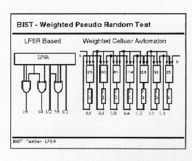 Weighted pseudorandom test
1. Random pattern has low testability because there are many random pattern resistant faults such
as the output of an and gate tree.
2. One way to cope with the problem is to change the probability of 1s or weights of each
inputs.
3. For LFSR, one can use logic gates to change the weight. Example, as shown in the slide.
4. For CA, with the hybrid structure, cells of different types, one can change the weights of
each inputs. However, it is difficult to determine the weights. Example, as the slide.
Figure 1. Lecture Handout - Slide and Note
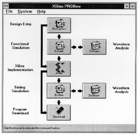
Figure 2. Lab FPGA Environment up
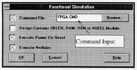
Figure 3. Step-By-Step Lab Instruction up
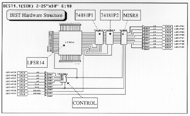
Figure 4. Test Circuit and Test Environment Setup up
 Back to Table of
Contents
Back to Table of
Contents