FERLIN, Edson Pedro1 & ELEUTERIO, Marco Antonio M.2
Pontificia Universidade Catolica do Parana, Laboratorio de
Logica Programavel - Eng. Computacao,
Caixa Postal 6432 Cep. 80.020-010,
Curitiba-Parana-Brasil,
1ferlin@ccet.pucpr.br,
2
marcoa@ppgia.pucpr.br
Abstract: The current technological stage has contributed to the adoption of new techniques and tools in teaching Engineering. This way, the Pontifical Catholic University of Parana (PUC PR) set up an agreement with AlteraTM , through its University Program, where programmable devices, as well as its corresponding development environment were supplied for academic use. In this partnership, the Computer Engineering course is introducing these tools as part of its graduate projects.
By using programmable devices in the digital systems design course, we could observe a high impact in decreasing the development and prototyping time when compared to the development using conventional ICs. The whole performance in teaching digital systems design was improved due to the simplicity in changing the original design and rapidly testing the programmable devices.
Another indirect benefit of using programmable logic in Engineering courses is that the students receive new qualifications in addition to the traditional digital systems design curriculum. By using this technology in the graduate course, the students also get new opportunities in their future carrier.
Keywords: programmable logic devices, VHDL, AHDL, digital design, development environment, hardware description language
The current technological stage has contributed to the adoption of new techniques and tools in teaching Engineering. This way, the Pontifical Catholic University of Parana (PUC PR) set up an agreement with AlteraTM , through its University Program, through which programmable logic devices (PLDs), as well as the whole development environment (MAX+PLUS IITM) [ALT 97]; were made available for academic use.
By using this tool, the Computer Engineering course has improved the technological level of some of its disciplines, such as Digital System Design and Microprocessors, where the students take great advantage of state-of-art tools available on the market [FER 98].
In order to support the project development with programmable devices, the Programmable Logic Laboratory was created. This laboratory is responsible for maintaining the physical resources, such as equipment and devices, as well as the technical staff which also develops using PLDs and generates technical and academic documentation to serve as research material for other development activities with programmable devices.
The knowledge and experience acquired in the laboratory is stored in the form of technical reports, papers, seminars and conferences.
The laboratory is composed of 26 PCs, 6 of which used by the researchers and 20 of which used for practical classes and experiments. All PCs are networked under Windows NT and run the Altera's MAX+PLUS II as the development environment.
The laboratory also provides various equipment for the projects:
digital osciloscopes;
digital boards;
multimeters;
EPROMs programmers/erasers;
power supplies.
To support the development of the experiments, we use the Educational Kits - Design Laboratory Package, made up of: UP 1 - Education Board, ByteBlaster Programming Cable and Hardlock for MAX+PLUS II software package. The Education Board is supplied with 2 programmable logic devices (PLDs) which can be used in conjunction or separately, as well as the power supply and recording hardware. This significantly reduces the prototyping time.
The laboratory has two professors/researchers who develop and conduct projects as well as students of the final year of the course who carry out their graduate project by using programmable logic devices.
In 1998, 8 students worked in the laboratory; 5 of which were developing their graduate projects and 3 of them were involved in complimentary activities.
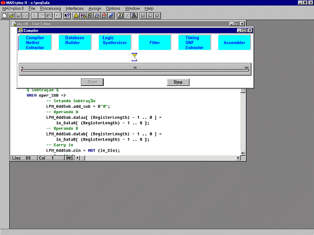
This software package (see figure 1) is a powerful toll for the development of digital designs using programmable logic devices. It manages all the development process, from the design up to the device programming stage. This includes various intermediate processing steps, such as compilation, circuit simulation and parameter checking (e.g. delay times).
Figure 1. MAX+PLUS II - Windows 95 interface
In figure 2 we can clearly see the 3 development stages in the development of a project: Project Input, Project Compilation and Device Programming/Verification.
MAX + PLUS II software can be divided in several modules, which enables the designer to choose the better way to realize its project. For example, one can either use a graphical editor for placing each component and defining its associated connections or can use a text editor through which a description of the circuit is entered in VHDL VHSIC (Very High Speed Integrated Circuit) Hardware Description Language form [ALT 96] or AHDL (Altera Hardware Description Language) [ALT 95]).
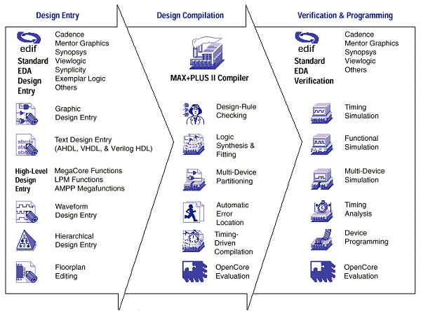
Figure 2. MAX+PLUS II Project Environment
MAX + PLUS II is an extremely flexible and versatile tool for the digital systems designer. A project developed under MAX+PLUS passes through various stages before reaching its final implementation. The process starts in the Design module (Text Design Entry, Wave Form Design Entry, Graphic Design Entry, among others), passes through the Compilation module (code generation for further programming) and finally the Verification and Programming stage (MAX+PLUS Programmer), where the final verifications are carried out and the programming of the Altera chip takes place.
The programming of the devices is of the ICR type (In-Circuit Reconfigurability) or ISP (In-System Programmability) [ALT 97], i.e., it takes place with the device on board. The recording time depends on the storage element type (memory) that the device uses for storing the data. The storage element can be either an EEPROM (Electrically Erasable Programmable Read-Only Memory) [CHR 97], which stores the data regardless of the power supply or an SRAM (Static Random-Access Memory) [CHR 97], which stores the data as long as the power supply is applied to the device.
Programmable logic devices can be divided in two categories: one-time programmable and re-programmable. The one-time programmable category includes the PLAs (Programmable Logic Arrays), in which programming is done via internal connection burning. The re-programmable category includes the PLDs (Programmable Logic Devices), CPLDs (Complex-Programmable Logic Devices) e FPGAs (Field-Programmable Gate Array), which can be programmed many times, thus allowing reusing them in other projects.
These devices have specific features [FER 98] that differ them from the traditional devices and make them attractive for digital designs.
There are two ways of programming such devices: by means of a textual description such as VHDL and AHDL or by means of a graphical editor which provides a set of logical elements (e.g. flip-flops, logic gates) and connections. One can also import a schematics file generated by other compliant software (e.g. OrCad).
When using VHDL or AHDL, the designer can choose among three types of programming:
Structural (interconnection of logical components generally using logical elements (logic gates) and bi-stable circuits (flip-flops)),
Data Chain (where each output signal is expressed through boolean equations)
Behavioral (based on algorithms, where the execution is conditioned at the occurrence of an event, e.g. a rising edge of a clock signal [OLS 98].
We have developed three projects in our laboratory using the MAX-PLUS environment and the programmable logic devices: a keyboard controller, an I/O interface and a didactic CPU.
The objective of this project is the development of a digital circuit using Altera's PLDs which allows direct interface between a PC standard keyboard and a general purpose microprocessor-based system.
This interface converts the serial mode signal generated by the PC keyboard to a parallel signal which will be made available to the data bus of a microprocessor-based system. Besides the serial-to-parallel conversion, this interface also performs the mapping from the keyboard code to the ASCII (American Standard Code for Information Interchange) format..
The objective of this interface is to use highly available and low-cost PC keyboards as data input devices for dedicated microprocessor-based systems.
The I/O interface project is intended to control two 8-bit I/O devices by using a PC compatible microcomputer. This interface is connected to the computer through the standard ISA (Industry Standard Architecture) bus.
This project is composed of three distinct functional blocks implemented in a single PLD. The first block is responsible for the address decoding which activates the two remaining blocks which in turn control the data input/output through the bus.
This circuit provides two 8-bit I/O ports, to which can be connected parallel devices, such as A/D and D/A converters for digital and analog data acquisition.
This CPU was developed for academic purposes and serves as a reference for the Digital Systems Design and Microprocessor courses.
The circuit is a 4-bit CPU composed of 3 functional blocks: Data Flow (ALU - arithmetic and logic unit, registers and data bus), Control Unit (control memory, activation signals and special function registers (PC - Program Counter, IR - Instruction Register, etc) and Program Memory.
This project was implemented using 2 PLDs which are part of the Altera's Education Board.
We are gradually introducing programmable logic in the computer engineering course by first applying it to the graduate courses and then motivating graduate projects to deal with Altera's environment and programmable devices. By using this technology within the course, we observed an improvement both in the quality of the practical experiments and the motivation level that the students have shown about digital design. Prototyping a digital system has never been so easy and cost effective. The students can describe their circuits in a declarative language (or by means of a schematics), apply different input signals and observe the behavior of the digital system (e.g. delay times) through simulation. This has clearly increased the students' understanding about the digital systems domain and has also improved the performance of the related courses.
[ALT 95] - ALTERA CORPORATION. MAX+PLUS II - AHDL. California-USA: Altera, 1995.
[ALT 96] - ALTERA CORPORATION. MAX+PLUS II - VHDL. California-USA: Altera, 1996.
[ALT 97] - ALTERA CORPORATION. MAX+PLUS II - Getting Started. California-USA: Altera, 1997.
[CHR 97] - CHRISTIANSEN, DONALD. Electronics Engineers Handbook. Fourth Edition. New York-USA: IEEE Press, 1997. pp. 11.55 - 11.65.
[FER 98] - FERLIN, EDSON PEDRO & ELEUTERIO, MARCO ANTONIO M., Vantagens na Elaboracao de Projetos Digitais Utilizando Dispositivos Logicos Programaveis". Anais. IV Simposio de Pesquisa e Extensao em Tecnologia. Natal-RN-Brazil: UFRN, 1998. pp. 97 - 99.
[OLS 98] - OLSZEWSKI, P. Logica Programavel - Novas Tendencias. in: Elektor Eletronica & Microinformatica. Editado por Ferreira & Bento, No 159. Marco de 1998. pp. 25 - 27.