SMART SENSOR TECHNOLOGY: A MULTI-DISCIPLINARY
COURSE
SEQUENCE
We have developed a unique course sequence on smart sensor and device technology. This course sequence is derived from our research on wide band gap semiconductor, magnetic multilayers and graded ferroelectric materials and sensor device applications. This multi-disciplinary-industrial collaborative work is combined with current device materials and structures research to form a comprehensive two semester hands-on course on sensor development and VLSI Technology. Students study the physics and technology of sensors and related devices, the associated electronics needed to drive the device and process information, and the techniques used for device fabrication. Students design, fabricate, and characterize sensor devices in a teaching laboratory and design associated VLSI circuitry for hybridization with the device. An outline of the research, smart sensors course sequence, and VLSI design integration is reported. This project is funded by a National Science Foundation Combined Research and Curriculum Development (CRCD) program grant.
The technology of electronic and photonic materials, devices and associated interactive electronics are of critical importance in United States industries and government laboratories. Among the most important areas of research is the integration of electronic processing combined with sensor devices (smart devices). Sensor research presents a strong multi-disciplinary challenge. The research and educational need in this area is to provide a more effective integration of very large scale integration (VLSI) circuitry with sensors. We have developed a combined research-curriculum initiative, funded by the National Science Foundation, which uses existing materials development research for microelectronics devices in combination with integrated electronic circuitry to make "smart devices". The devices covered in this course include standard state-of-art sensor devices as well as pioneering prototype sensors from wide band gap semiconductors, pyroelectric materials and magnetic multilayers. The course materials are developed from our current research projects as outlined in Table 1. The course includes a hands-on lecture Laboratory sequence using existing experimental methods to design and fabricate prototype smart devices. A VLSI/Device Simulation Laboratory has been developed for the course sequence to allow students to design and simulate the devices before fabrication. Sensor device design and construction is followed by VLSI circuitry developed to integrate with the working device. An emphasis is placed on design aspects and teamwork in completing the projects. This type of integrated technology where students are trained in device design, fabrication and integrated circuitry is what industries need to be competitive. For this reason, a close collaboration with local industries has been established to enhance the course curriculum and aid in the course design. Industrial participants include Ford Motor Company in the area of special automotive sensors such as high temperature exhaust sensors and General Motors in the area of collision avoidance sensor systems. The goals and objectives, educational methodology, curriculum design, details of industrial interactions and accomplishments are outlined in this paper.
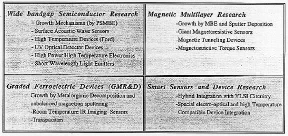
Table 1- Summary of Research Activities. up
Sensor Physics and Technology
In order to implement our smart sensor and device research into the engineering curriculum we have developed a course sequence which details the solid state device (and physics) aspects of sensors and related devices and analog VLSI design as a building block for sensor integration'. Students begin by learning about the basic types of sensors and related devices currently used and under investigation2. Sensor device design strategies are discussed in the context of current applications and future needs- a mixture of generic sensor devices, specific state-of-the-art sensors, novel new possibilities in smart sensors and integrated devices. The specific physical measurands are correlated to particular devices and the fabrication techniques employed in device fabrication are discussed. This initial introduction to sensor technology is followed by a team project where students design a sensor to meet a particular application. Device fabrication methods are planned and a block diagram of the integrated electronics associated with the device is designed. Following their design projects, the students will work on a sequence of VLSI design experiments to learn the basic tools necessary for a final comprehensive project combining the fabrication and characterization of a sensor, the development of associated VLSI circuitry, hybridization of the sensor and VLSI circuit, packaging, and finally testing the devices. The sensor physics and technology course sequence is outlined in Table 2.
| Measurands
|
Acoustic Sensors
|
Magnetic Sensors
|
Mechanical Sensors
|
|
Radiation Sensors
|
Thermal Sensors
|
Chemical Sensors
|
Biosensors
|
Table 2. Outline of material covered in the two course sequence on smart sensors an integrated devices.
VLSI Design
Each sensor has its own particular sensing application and output3. Some sensors produce an output voltage, current, a resistance or capacitance. The smart sensor system must integrate this sensor output on one chip, without external components as illustrated in Figure 1.
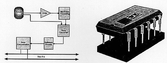
Figure 1. Diagram of Sensor system with integrated electronics.
The VLSI integration portion of the course sequence begins with a block diagram of the circuitry needed for the fabricated sensor device (based on sensor characterization). The VLSI curriculum consists of one hour lecture and three hours laboratory a week. The VLSI portion begins by building on basic concepts to familiarize students with the software and design strategies. The following is an outline the VLSI material covered in the two-course sequence:
1. CMOS Switch -- Introduces the student to the process of custom layout using Mentor Graphics software package. The students learn how to layout a standard cell which will be part of a standard cell library for analog VLSI design of more complicated circuits. The students learn spice netlist extraction, simulation and symbol creation for the cell.
2. Multiplexer - CIF -- Introduces the students how to interpret a CIF file. The students actually use the CIF file generated for the CMOS Switch to implement a 2 to 1 analog multiplexer. It introduces the concept of routing channels for standard cells. The resulting CIF is converted back to layout for simulation and netlist extraction.
3. 2 to 1 Multiplexer - Automated Layout -- Introduces the Mentor Graphics automated layout tools. The students use schematic diagram to interconnect two CMOS Switch symbols to create an analog 2 to 1 multiplexer. The concept of compacting the resulting layout is introduced, the result should be very close to the manually created CIF of 2 to 1 multiplexer.
4. Preparation for Fabrication--Introduces the students the steps needed for successful submission of their project to MOSIS. CIF file created by Mentor Graphics must be modified to conform with MOSIS requirements such as: scaling factor, elimination of redundant layers, mapping of Mentor Graphics layers to MOSIS layers, CIF file checksum using checksumcif, etc. The syntax for e-mail submission is presented.
5. Project I -- Introduces logic design using analog CMOS switches based on Shannon expansion theorem. It demonstrates that the 2 to 1 Multiplexer can be used to implement any two variables logic gate. The MUX 4 to 1 is shown to be a programmable two variables universal logic gate. Any circuit design using analog switches, being bi-directional devices, the resulting circuit is also bi-directional. That is implementing a MUX 4 to 1 also simultaneously implement a DEMUX 4 to 1 as well as a programmable two variables universal logic gate. Based on these, each group is assigned to implement a MUX 4 to 1 and any digital logic modules such as encoder, decoder, code converter, arithmetic logic unit etc.
6. Resistor Layout -- Introduces the proper way of laying out resistor of a given value and as a standard cell. It introduces how to interpret the resistive electrical process parameter of each layer.
7. Capacitor Layout -- Introduces the proper way of laying out capacitor of a given value and as a standard cell. It introduces how to interpret the capacitive electrical process parameter of between layers.
8. Large Transistor Layout - Introduces how a transistor with large W/L specification can be achieved using parallel interconnection of transistors with smaller W/L. This technique made it possible to create standard cell (cell with the same overall height) for possible automatic layout of analog chip.
9. NMOS Inverter with Resistive Load--Introduces the simplest gain stage consisting of one NMOS transistor with resistive load. The gain is shown to be very limited and it occupies larger area, since passive resistor (<25K) using polysilicon requires large area.
10. NMOS Inverter with NMOS load - Introduces another simple gain stage using two NMOS transistors. The resistive load is replaced by an NMOS transistor. This configuration has a rather low gain but it is process independent.
11. NMOS Inverter with PMOS Current Load - Introduces a simple gain stage using NMOS transistor with PMOS current load. The gain stage is much higher than the previous stages.
12. CMOS Inverter -- Introduces complementary inverter gain stage consisting of NMOS and PMOS transistors. Each transistor acts as a driver and as a load of the other transistor. The advantage is high gain and no quiescent current. That is, no power drain at operating point.
13. Current Mirror and Voltage Divider Circuit Introduces the concepts of current mirrors for generating the various current sources or sinks needed by the various gain stages. The voltage divider is used to achieve any voltage reference value. This voltage reference can then be used to create current reference used by current mirrors.
14. Differential Amplifier-Introduces the differential input stage of an Opamp circuit. It is shown that differential input stage with current mirror load achieved self biasing. This is not the case in all the simple gain stages discussed previously, where the bias is very critical that a small error in the bias can completely put the gain stage in saturation region or no gain.
15. Opamp Design - Introduces the concept of feedback to achieve a stable oparnp circuit. Opamp consists of two gain stages and one buffer stage. The three stages represent a third order system, which for stability requires compensation. The compensation is achieved by a compensation capacitor which also limit the slew rate and gain bandwidth of the opamp due to Miller effect. The buffer sta~e is used to achieve a low output impedance opamp.
16. Opamp Special Circuits -Introduces various opamp special circuits that are important for sensor signal processing. Some circuits that are covered are: State variable universal filter, which simultaneously provide 2nd order low-, high-, band-pass-, and band-reject- filter; Precision break point circuits, used to approximate any non-linear functions such as absolute value, square etc.; Voltage to current converter, for converting sensor for remote sensing applications, Multiplying circuits for detecting phase shifting in surface acoustic wave (SAW) devices etc.
Hands-on Integrated Sensor Projects Once students have the theoretical background in sensor and VLSI technology students begin their final projects. These projects consist of fabricating the sensors in our research laboratory, characterizing the device, and designing the VLSI circuitry to hybrid with the sensor. Students work to fabricate a sensor. Current sensor projects include a surface acoustic wave biosensor, a giant magnetoresistance tunneling sensor, an infrared pyroelectric sensor, and an ultra violet optical sensor. The projects are chosen to cover most of the different sensor classifications at a state-of-the-art level. The associated signal processing VLSI circuit is then designed, simulated and submitted for fabrication to MOSIS. A library of standard analog cells is currently being developed to speed up the design process.
We have developed a two semester course sequence on smart sensors and integrated devices that builds on our current research thrust areas. This course sequence covers general sensor physics and technology as well as new and novel state of the art sensor design. Students work on a design project to fabricate and test an actual sensor device. Design strategies are covered for VLSI implementation and hybridization of a fabricated sensor with associated electronic control and communications circuitry. The goal of the course sequence is to use our research and facilities in smart sensor development to give students a comprehensive background in the art and science of sensor and device technology, design, fabrication and integration.
This material is based upon work supported by a National Science Foundation- Combined Research-Curriculum Development Program Grant EEC-9420568.
1. Handbook of Modern Sensors, J. Fraden, 2nd ed., Americat Institute of Physics ( 1996).
2. R.M. White, 'EEE Trans. Ultrason. FeIToelec. Freq. Contr.', UFFC-34, 124(1987).
3. Intellegrent Sensor Systems, R. Ohba, Chichester: John Wiley, (1992)
 Biological (biomass, identities, concentrations
 Back to Table of
Contents
Back to Table of
Contents